General Description
The RT4822 is a boost regulator designed to provide a minimum output voltage from a single-cell Li-Ion battery or two alkaline battery series, even when the battery voltage is below system minimum. Quiescent current in shutdown mode is less than 1µA, which maximizes battery life.
Performance Specification Summary
The boost conveter has an input voltage range from 1.8V to 5.5V, and the output voltage range is from 3.15V to 5.5V. It can operate in force bypass mode and boost mode. And the power-on inrush current and current limit are implemented serval setting for difference application. The RT4822 is available in a WL-CSP-9B 1.3x1.2 (BSC) package.
Table 1. RT4822WSC Evaluation Board Performance Specification Summary
|
Specification
|
Test Conditions
|
Min
|
Typ
|
Max
|
Unit
|
|
Input Voltage Range
|
|
1.8
|
--
|
5.5
|
V
|
|
Output Current
|
VIN > 3V, VOUT = 5V
|
0
|
--
|
1.5
|
A
|
|
Default Output Voltage
|
|
--
|
5
|
--
|
V
|
|
Operation Frequency
|
|
3
|
3.5
|
4
|
MHz
|
|
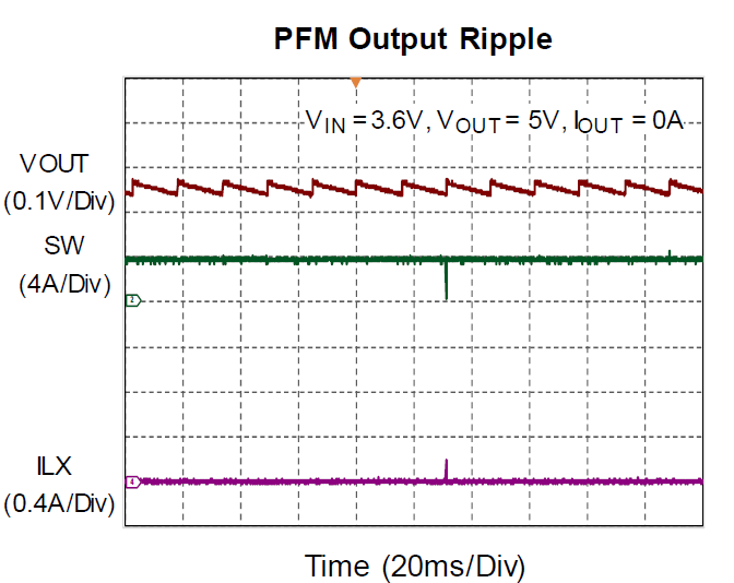
Output Ripple Voltage
|
VIN = 3.6V, VOUT = 5V, IOUT = 0.5A
|
--
|
40
|
--
|
mVp-p
|
|
Line Regulation
|
IOUT = 0.5A, VIN = 1.8V to 4.8V, VOUT = 5V
|
--
|
±1
|
--
|
%
|
|
Load Regulation
|
VIN = 3.6V, IOUT = 0.2A to 1A, VOUT = 5V
|
--
|
±1
|
--
|
%
|
|
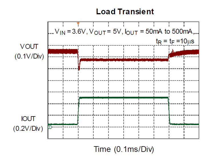
Load Transient Response
|
VIN = 3.6V, VOUT = 5V ,IOUT = 50mA to 500mA
|
--
|
±3
|
--
|
%
|
|
Maximum Efficiency
|
VIN = 3.6V, VOUT = 5V, IOUT = 0.6A
|
--
|
93
|
--
|
%
|
Power-up Procedure
1. Connect input voltage (1.8V < VIN < 5.5V) to VIN pin.
2. Setting BOOST enable selection by CHIP_EN. (setting 0x05[0] by I2C)
3. Setting BOOST pre-charge current and BOOST_LIMIT for power on inrush current. (setting 0x00 by I2C)
4. To enable Boost converter by external EN pin or 0x05[5].
5. To connect an external load to output and verify the output voltage versus applied current.
Output Voltage Setting
The output voltage set by internal register in the following I2C table.
|
Addr
|
Reg Name
|
Bit
|
Bit Name
|
Default
|
Type
|
Description
|
|
0x02
|
BOOST_VOUT
|
7
|
Reserved
|
0
|
RW
|
Reserved
|
|
6:0
|
BOOST_VOUT
|
1101011
|
RW
|
Boost output voltage can be set voltage from 3.15V to 5.5V with 25mV/step.
0000000 to 0100001: 3.15V
…
1101011: 5V (default)
…
1111111: 5.5V
|
Detailed Description of Hardware
Headers Description and Placement
Carefully inspect all the components used in the EVB according to the following Bill of Materials table, and then make sure all the components are undamaged and correctly installed. If there is any missing or damaged component, which may occur during transportation, please contact our distributors or e-mail us at evb_service@richtek.com.
Bill of Materials
|
Reference
|
Count
|
Part Number
|
Description
|
Package
|
Manufacture
|
|
CN1
|
1
|
CHEB254S006-CF1043
|
I2C
|
|
Cherng Weei
|
|
C1
|
1
|
EMK325BJ476KM-T
|
47µF/16V/X5R
|
1210
|
TAIYO YUDEN
|
|
C2
|
1
|
GRM155R60J475ME47
|
4.7µF/6.3V/X5R
|
0402
|
Murata
|
|
C4
|
1
|
0603X106M6R3CT
|
10µF/6.3V/X5R
|
0603
|
WALSIN
|
|
L1
|
1
|
DFE252012F-1R0M=P2
|
1.0µH/3.3A
|
2.5x2.0x1.2mm
|
Murata
|
|
R1, R2
|
2
|
WR06X2201FTL
|
22k/0603
|
0603
|
WALSIN
|
|
U1
|
1
|
RT4822WSC
|
Step-Up DC-DC Converter
|
WL-CSP-9B 1.3x1.2 (BSC)
|
RICHTEK
|
Typical Applications
EVB Schematic Diagram
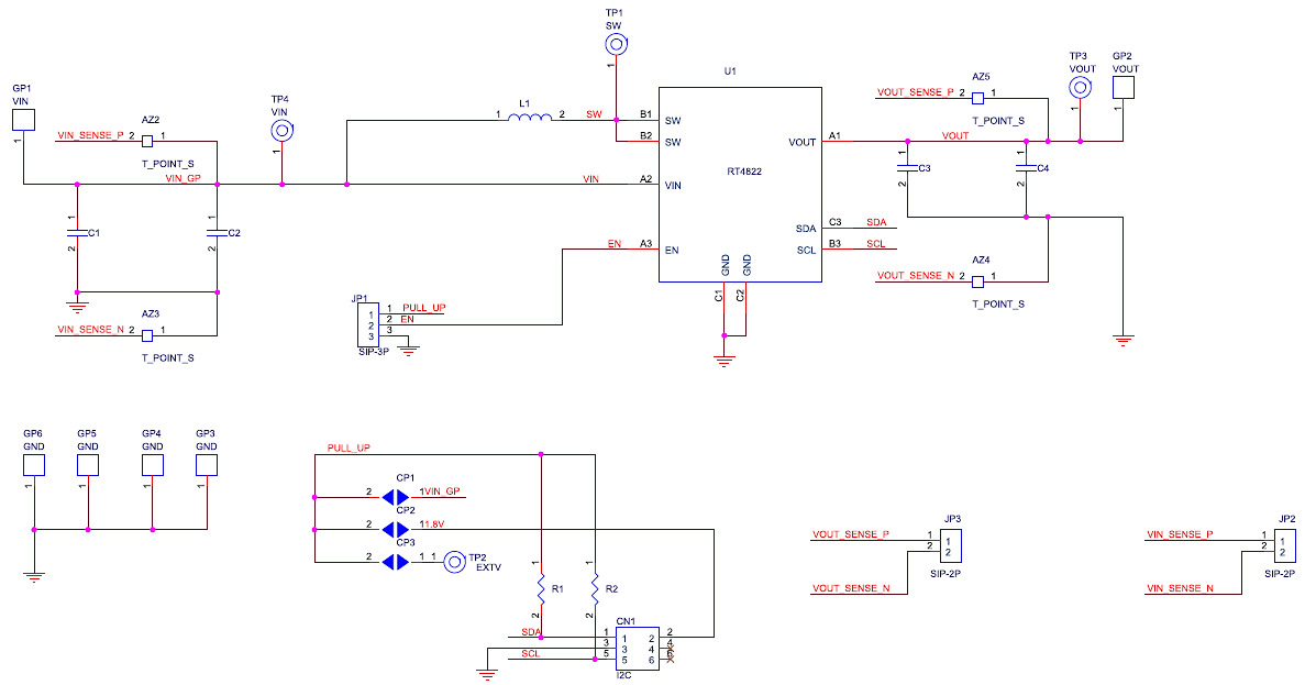
1. C1 is placed on input side, and the capacitors are design for long wire effect. If input source is close RT4822 then the capacitors are optional.
2. C4 is placed on output side, and the capacitor is optional for output voltage ripple improvement.
Measure Result
|
Output Ripple Measurement
|
Load Transient Response
|
|
|
|
|
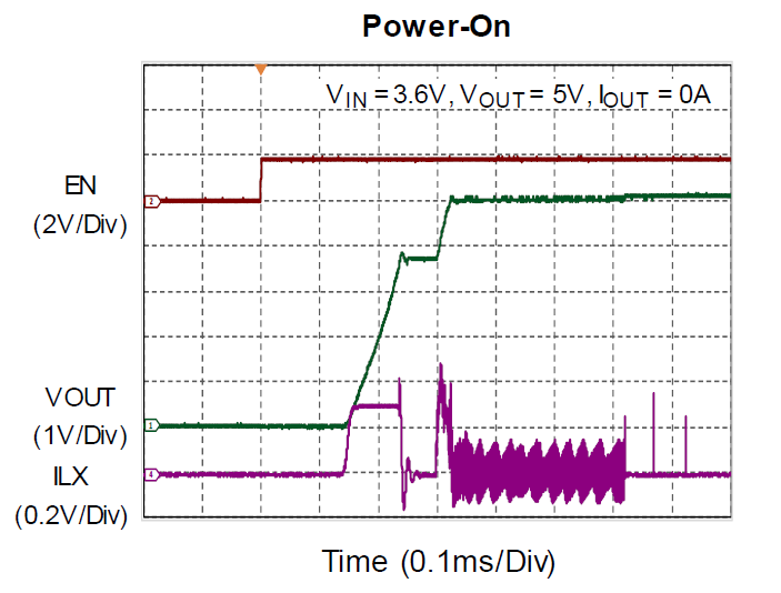
Power On from EN
|
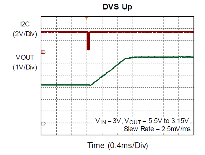
DVS up
|
|
|
|
|
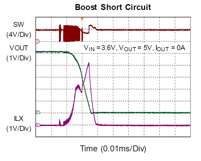
Short Circuit Response
|
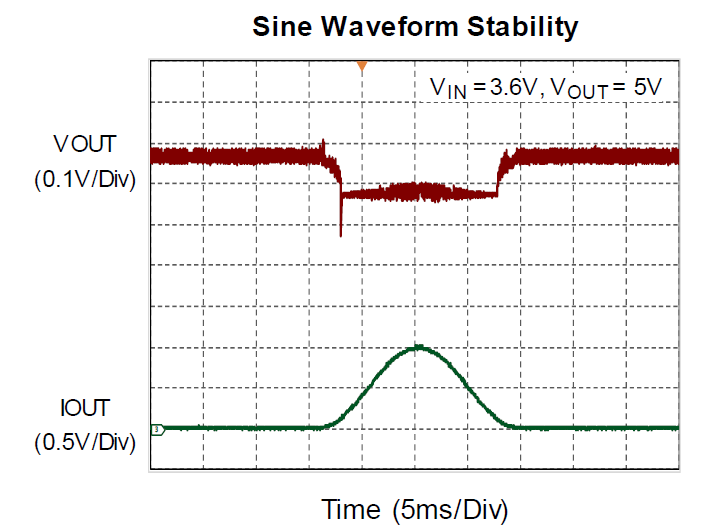
Sine Waveform Stability
|
|
|
|
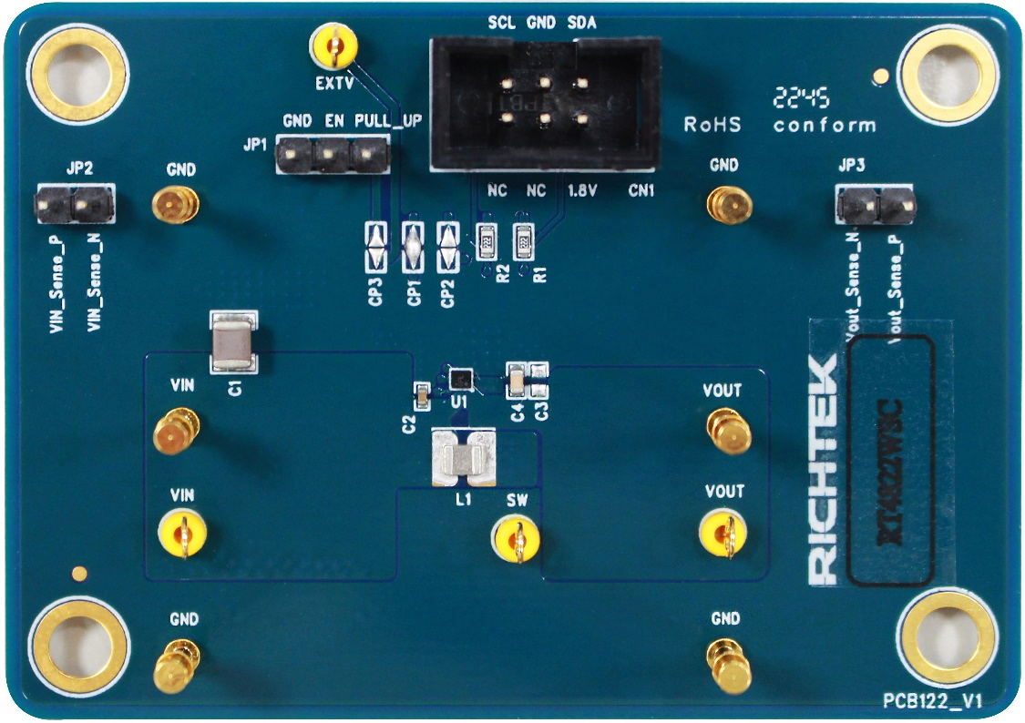
Evaluation Board Layout
Figure 1. Top View (1st layer)

Figure 2. PCB Layout—Inner Side (2nd Layer)
Figure 3. PCB Layout—Inner Side (3rd Layer)
Figure 4. Bottom View (4th Layer)